Soitec Announces Industry's First Four-Junction Solar Cell for Concentrator Photovoltaic Systems, Entering Industry's Roadmap at World-Class Level with 43.6% Efficiency
Technology innovation opens the path to competitiveness breakthrough in PV industry
BERNIN, France, May 22, 2013--
Soitec (Euronext), a world leader in generating and manufacturing revolutionary semiconductor materials for the electronics and energy industries, announced today the industry's first four-junction solar cell device, which works under concentrated sunlight, putting the company on the solar-energy industry's technology roadmap at a world-class level of an outstanding 43.6 percent efficiency. This technology development - made possible through strong collaboration between solar cell device and epitaxial growth centers of expertise combined with Soitec's decades-long leadership in substrate-bonding and layer-transfer technologies - validates the unique roadmap enabling, thanks to the four junctions structure to target the 50-percent efficiency level. This roadmap marks a major competitiveness breakthrough in the photovoltaic industry.
Soitec's four-junction solar cell has achieved today a peak efficiency of 43.6 percent, as confirmed by the Fraunhofer ISE Calibration Laboratory. This measurement was achieved at a concentration level of 319 (319 suns). The new cell has demonstrated more than 43 percent energy-generating efficiency over a concentration range between 250 and 500.
Today's triple-junction solar cells used in commercial concentrator photovoltaic (CPV) modules in real-world applications are approaching their physical limits in converting sunlight into renewable energy. Soitec's four- junction cell is designed to increase the conversion efficiency of commercial CPV systems to the highest level ever achieved by any photovoltaic technology. Based on the initial results obtained using very few integration runs, Soitec is well positioned at the front of the efficiency race.
The innovative four-junction cell uses two new, highly sophisticated dual-junction sub cells grown on different III-V compound materials, which allows optimal band-gap combinations tailored to capture a broader range of the solar spectrum. This maximizes energy-generating efficiency. Soitec leverages its proprietary semiconductor-bonding (Smart Stacking™) and layer-transfer (Smart Cut™) technologies, which have been used in volume production by the global semiconductor industry for decades, to successfully stack non-lattice-matched materials while also raising the possibility of re-using expensive materials.
The new cell was developed in collaboration with the Fraunhofer Institute for Solar Energy Systems (ISE) in Freiburg, Germany, and the Helmholtz-Zentrum f�r Materialien und Energie in Berlin, which developed and deposited III-V epitaxial layers on new base materials as well as fabricating and characterizing the device. CEA-Leti, France's research institute for electronics and information technologies, also actively participated in the project and contributed its expertise in mechanically strong, electrically conductive and optically transparent bonding interfaces as well as layer-transfer engineering of III-V compound materials.
"Boosting efficiency levels is a key step in outperforming the economics of conventional PV. This great achievement brings strong value to our solar division and validates our strategy and business model in the solar market," said Andr�-Jacques Auberton-Herv�, CEO of Soitec. "Through our collaboration with the Fraunhofer and the Leti, two world-class R&D partners, our own leadership experience in materials and bonding technologies as well as our CPV commercial experience, we have been able to achieve this major advancement in a very short time. This represents a major proof-of-concept, on track to demonstrate a concentrated solar cell with 50% efficiency as soon as 2015."
About Soitec:
Soitec is an international manufacturing company, a world leader in generating and manufacturing revolutionary semiconductor materials at the frontier of the most exciting energy and electronic challenges. Soitec's products include substrates for microelectronics (most notably SOI: Silicon-on-Insulator) and concentrator photovoltaic systems (CPV). The company's core technologies are Smart Cut™, Smart Stacking™ and Concentrix™, as well as expertise in epitaxy. Applications include consumer and mobile electronics, microelectronics-driven IT, telecommunications, automotive electronics, lighting products and large-scale solar power plants. Soitec has manufacturing plants and R&D centers in France, Singapore, Germany, and the United States. For more information, visit: http://www.soitec.com.
Featured Product

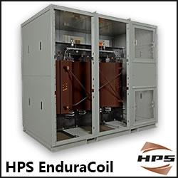
HPS EnduraCoilTM Cast Resin Medium Voltage Transformer
HPS EnduraCoil is a high-performance cast resin transformer designed for many demanding and diverse applications while minimizing both installation and maintenance costs. Coils are formed with mineral-filled epoxy, reinforced with fiberglass and cast to provide complete void-free resin impregnation throughout the entire insulation system. HPS EnduraCoil complies with the new NRCan 2019 and DOE 2016 efficiency regulations and is approved by both UL and CSA standards. It is also seismic qualified per IBC 2012/ASCE 7-10/CBC 2013. Cast resin transformers are self-extinguishing in the unlikely event of fire, environmentally friendly and offer greater resistance to short circuits. HPS also offers wide range of accessories for transformer protection and monitoring requirements.
